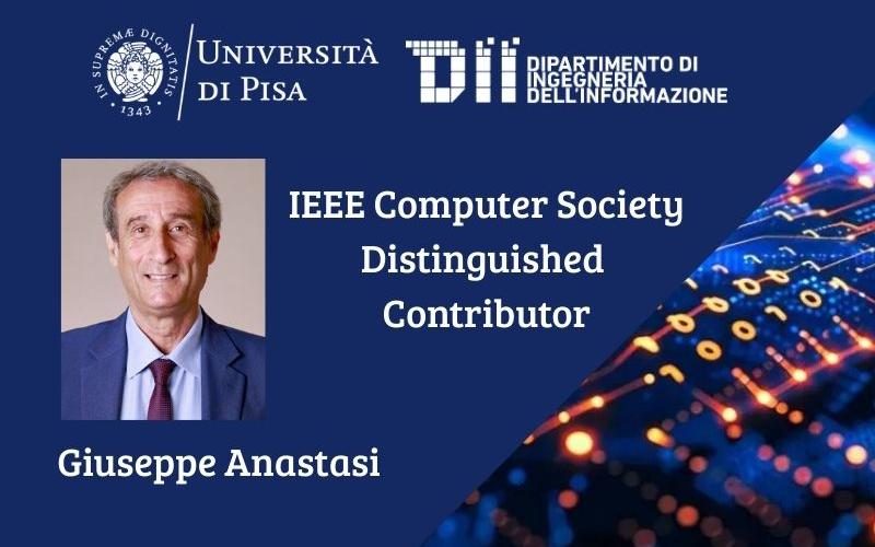
La nomina a Distinguished Contributor (DC) premia i membri e gli affiliati della Computer Society che hanno apportato contributi tecnici significativi e continuativi alla IEEE Computer Society, alla...
Leggi tutto
DII Talks: Drawing devices on paper with van der Waals materials - Andres Castellanos-Gomez
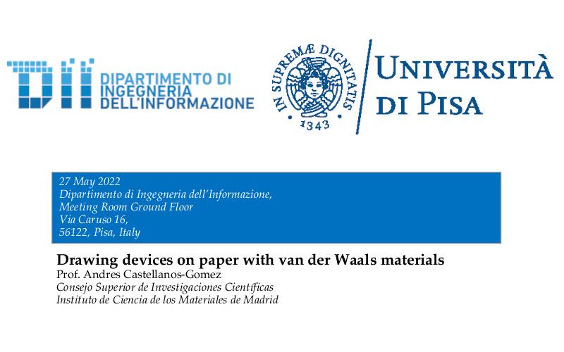
27 Maggio 2022
621
Andres Castellanos-Gomez
Consejo Superior de Investigaciones Científicas
Instituto de Ciencia de los Materiales de Madrid
Dipartimento di Ingegneria dell’Informazione,
Meeting Room Ground Floor
Via Caruso 16,
56122, Pisa, Italy
A big chunk of the price tag of electronic components is due to the cost of silicon wafer substrates. Although silicon is a highly abundant and cheap element, the transformation and processing from the raw material into high quality silicon wafers results very costly. In fact, the cost of silicon substrates constitutes ~1/3rd of the total cost of a memory chip and about ~1/10th of the cost of a high-end state of the art micro-processor. The societal, industrial and technological demands of ultra-low-cost electronic components has spurred the quests towards lower cost substrates. This has motivated a surge of works on paper-based electronics in the last years. In fact, paper substrates cost (~0.1 €/m2) is orders of magnitude lower than that of polymer substrates (PET ~2 €/m2 and PI ~30 €/m2) and crystalline silicon (~1000 €/m2). Despite the promises of paper-based electronics, there are several challenges to be solved. One of the major challenges is that the rough, fiber-based structure of paper makes it impossible to fabricate devices using conventional lithographic techniques. In this talk I will discuss our last works to integrate different van der Waals materials onto standard paper substrates [1-4].
[1] J Azpeitia et al. Materials Advances (2021)
[2] W Zhang et al. Applied Materials Today (2021) 23, 101012
[3] M Lee et al. Nanoscale (2020) 12 (43), 22091-22096
[4] A Mazaheri et al. Nanoscale (2020) 12 (37), 19068-19074
![]()
Dipartimento di Ingegneria dell'Informazione
Via G. Caruso 16 - 56122 - Pisa
Tel +39 050 2217511 - info@dii.unipi.it
PEC: ing.informazione@pec.unipi.it
Info Didattica: didattica@dii.unipi.it
P.I. 00286820501 - C.F. 80003670504